Product description
We develop a product helping the solution to the problem, and catch the needs of the times, and continue bringing about new value.
Product description
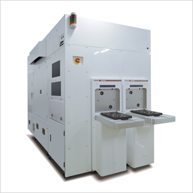
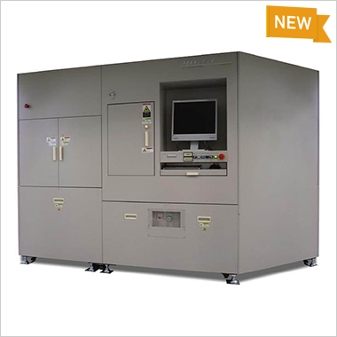
- Wafer Edge Inspection SystemRXW-1200
- The automatic inspection equipment to detect and classify wafer edge defects as well as to measure the size of required parts in the Si wafer or device manufacturing process
Semiconductor Manufacturing Process
Edge Grinding / Single Side Grinding / Double Side Polishing / Cleaning / Drying / Prime Wafer Final Inspection / Epitaxy, Silicon on Insulator / Deposition / Lithography / CMP / Edge Trimming / Pasting / Thinning
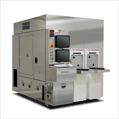
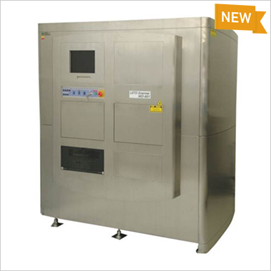
- Backside Macro Wafer Inspection SystemBMW-1200
- The inspection equipment with high sensitive detection of deficiency / contamination of wafer back side and with three-dimensional sharp measurement of extracted defects in device manufacturing process
Semiconductor Manufacturing Process
Deposition / Lithography / Etching / CMP
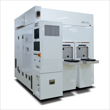
- Edge and Front / Back Surface Inspection EquipmentRXM-1200
- The inspection equipment to detect various kinds of deficiency of Wafer edge / both sides which occur is Si wafer manufacturing (Polishing / Epi) process
Semiconductor Manufacturing Process
Edge Griding / Single Side Grinding / Double Side Polishing / Cleaning / Drying / Prime Wafer Final Inspection / Epitaxy, Silicon on Insulator
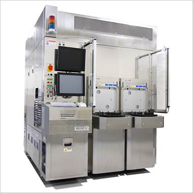
- Pinhole Defect Inspection EquipmentRXP-1200
- The automatic inspection equipment to detect pinhole defects using infrared light in the inside or on the back surface which occur in the Si crystal growth process
Semiconductor Manufacturing Process
Crystal Growth / Slicing / Single Side Grinding / Double Side Polishing / Prime Wafer Final Inspection
Please inform it of the question about the product then “inquiry”.